
Future nvidia gpus
in Graphics Cards
OP is referencing this: http://www.anandtech.com/show/7900/nvidia-updates-gpu-roadmap-unveils-pascal-architecture-for-2016
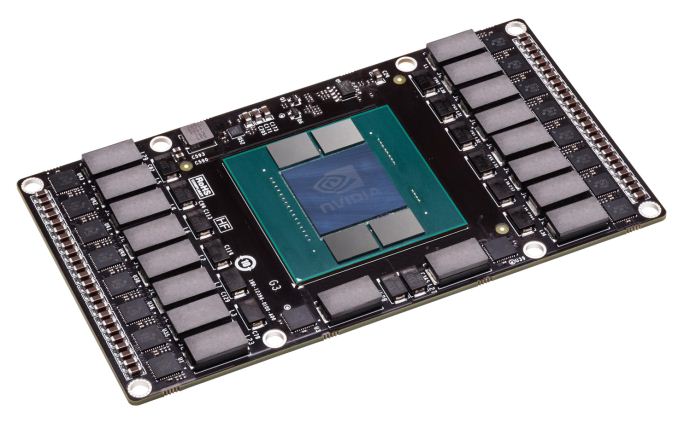
But the rabbit hole goes deeper. To pull off the kind of transfer rates NVIDIA wants to accomplish, the traditional PCI/PCIe style edge connector is no good; if nothing else the lengths that can be supported by such a fast bus are too short. So NVLink will be ditching the slot in favor of what NVIDIA is labeling a mezzanine connector, the type of connector typically used to sandwich multiple PCBs together (think GTX 295). We haven’t seen the connector yet, but it goes without saying that this requires a major change in motherboard designs for the boards that will support NVLink. The upside of this however is that with this change and the use of a true point-to-point bus, what NVIDIA is proposing is for all practical purposes a socketed GPU, just with the memory and power delivery circuitry on the GPU instead of on the motherboard.
NVIDIA’s Pascal test vehicle is one such example of what a card would look like. We cannot see the connector itself, but the basic idea is that it will lay down on a motherboard parallel to the board (instead of perpendicular like PCIe slots), with each Pascal card connected to the board through the NVLink mezzanine connector. Besides reducing trace lengths, this has the added benefit of allowing such GPUs to be cooled with CPU-style cooling methods (we’re talking about servers here, not desktops) in a space efficient manner. How many NVLink mezzanine connectors available would of course depend on how many the motherboard design calls for, which in turn will depend on how much space is available.
However, as i discussed with a friend of mine on skype, it is unlikely this will be the case once they actually roll around. I still think traditional PCIe slots will exist, and that NVLink will be adapted in another fashion. After all, that article is over 2 years old now, and we still have not reached the full limitations of PCIE 3.0 yet.

-
Topics
-
 0
0 -

Doctah ·
Posted in Peripherals0 -
 2
2 -

michaelb198 ·
Posted in Peripherals1 -

errorcode123_dindin1 ·
Posted in Graphics Cards2 -

Packhunter ·
Posted in Graphics Cards3 -
 12
12 -
 6
6 -

VirusDumb ·
Posted in Programming0 -

Jayraj ·
Posted in Power Supplies4
-
-
play_circle_filled

Latest From Linus Tech Tips:
Google’s Best Feature In Years - WAN Show June 5, 2026
-
play_circle_filled

Latest From ShortCircuit:
The coolest looking monitor. Period. - ASUS ROG display at Computex (Sponsored)


Create an account or sign in to comment
You need to be a member in order to leave a comment
Create an account
Sign up for a new account in our community. It's easy!
Register a new accountSign in
Already have an account? Sign in here.
Sign In Now